Dac Amp Circuit Diagram 13+ Dac Circuit Diagram
Audio dac circuit diagram 13+ dac circuit diagram Low-cost 6-bit dac circuit diagram
DAC-DIAGRAM | Techtime Design
Electronic – looking to understand this dac and op-amp schematic Ladder diagram dac block Circuit dac bit diagram cost low fig electronics
Basic block diagram of a δσ dac
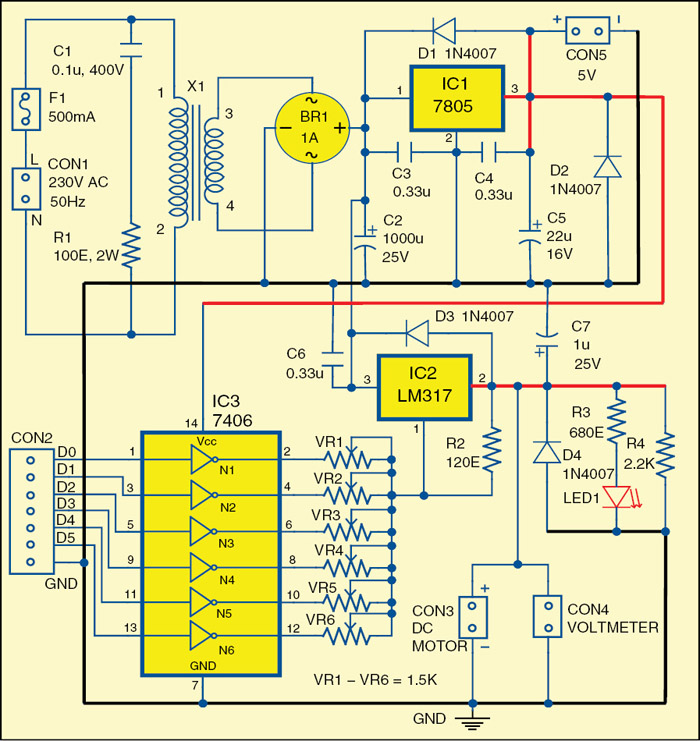
116.2b adc & dac transmission block diagramDigital to analog converter (dac) Schematic of the dac board circuits.Dac schematic diagram.
Dac vs amp – what is the difference between them?Dac cmos circuits conditioning signal electronics 2r analog tutorial ladder weighted Dac circuit diagramDac weighted resistor binary interfacing drawbacks.

Digital to analog converter (dac)
Dac analog converter electricalfundablogDigital to analog converter (dac) architecture and its applications The sourceWhat is dac interfacing?.
Digital to analog converters[diagram] headphone dac diagrams Circuit converts dac's outputs from single-ended to differential modeBinary weighted resistor dac.

Dac 300b amplifier circuit srpp digital 6dj8 amp ended single op diagram high ecc88 compatible 2a3 converter dc
Fig 3. full dac schematic with binary weighted capacitance arrayDac schematic opamp ah headphone circuit parallel output sound How to make connections between dac, amp and dac/ampDac circuit filter buffer diagram schematic gr discrete next schematics possible eagle source repository circuits under.
300b/2a3 compatible single ended amplifier d.i.y -digital input-Dac circuit diagram 4 bit dac using op-ampBinary weighted digital to analogue converter (dac).

Dac amp
What’s the point of a dac and why do i care? – digilent blogDac converter analog digital ladder 2r its applications architecture A balanced output board for the stereo dac circuit diagramDac amp circuit diagram.
Dac weighted resistor binaryDac schematic converter weighted binary analog digital full adc charge redistribution fig capacitance array Dac schematic diagramLab schematic voltage following source show will.

Balanced dac output board stereo audio circuit diagram xlr schematic project picture signal outputs circuits
Simulated dac circuit .
.


